Non-ideal Operational Amplifier properties
An ideal op-amp is a theoretical concept with infinite gain, infinite input impedance, zero output impedance, infinite bandwidth, zero input offset voltage, and zero input bias current. In real world an op-amp deviates from its ideal properties that approximates these, but with finite gain, high but not infinite input impedance, low (but not zero) output impedance, limited bandwidth, small offset voltage, and small bias currents due to manufacturing imperfections, making it suitable for real-world circuits. Some very important properties are described in the following section.
Gain-bandwidth product
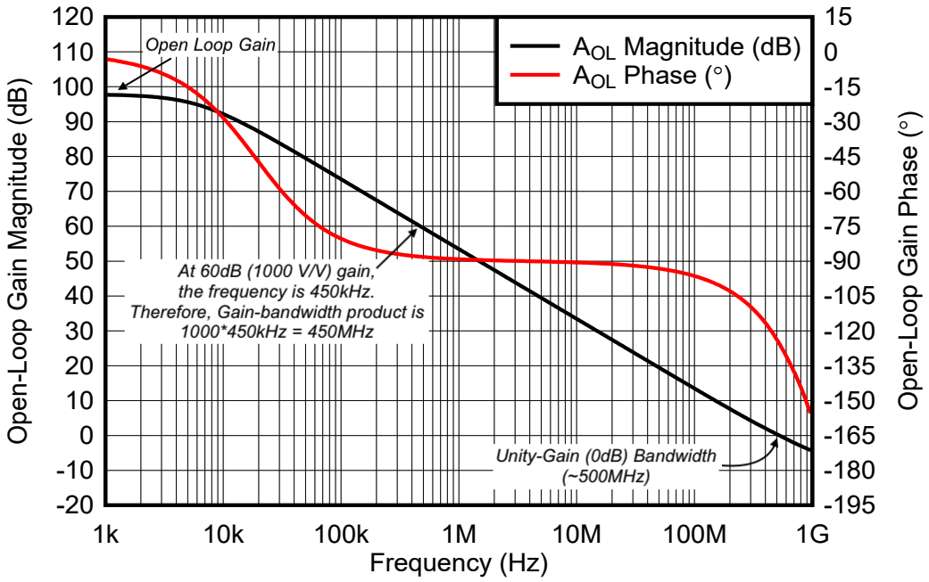
Gain bandwidth product is the multiplication of gain at a particular frequency. This is a constant number of an opamp. This number can vary from one opamp to another. Higher the gain bandwidth product number, the higher the speed and lower the harmonic distortion.
Open loop gain
Open loop gain is the gain of an opamp when it is not connected in any feedback loop. Usually, in an ideal opamp, this number is infinite. In real opamp, it is usually a very high number ranging from 20 dB (10 V/V) to 140 dB (107 V/V). It is usually measured at DC or very low frequency. Higher open-loop gain helps in suppressing systematic errors in the amplifiers. For precision amplifiers, the open-loop gain is near 120dB or above. For high-speed amplifiers, the open-loop gain is usually 70dB or above.
Unity gain bandwidth
It is the largest frequency when opamp has some gain (more unity gain). Anything above a gain of 1 V/V is called a gain, so 1 V/V is chosen as a cutoff gain.
Unity gain bandwidth can be different from gain-bandwidth product. Ideally, both should be equal. However in real world, to save power and provide better distortion while ensuring decent stability (gain and phase margin), the unity-gain bandwidth could be set lower than gain-bandwidth product. This is done by introducing pole-zero pair in the open-loop transfer function.
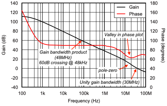
Due to this pole-zero introduction, we can also see a dip in phase plot. Due to pole-zero and where it is located the bode plot, the fine settling (e.g., 0.01%) can be long.
Phase and Gain Margin
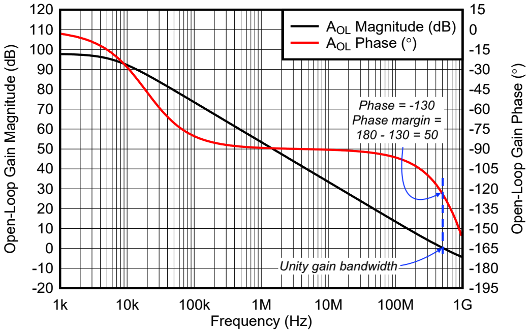
Phase margin can be derived from the bode plot using the method illustrated above. The unity gain-bandwidth has to be identified first. Following this, the phase needs to be mapped. The phase margin is the difference between phase and 180°
Slew rate
Slew rate is defined as the maximum rate of change of the output voltage concerning time. It is expressed in volts per microsecond (V/µs). The large signal step response is used to measure the amplifier's slew rate.
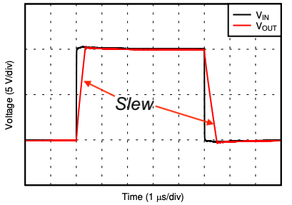
An opamp has an internal transconductance stage (gm) which takes the input differential voltage and converts it to an current, Itail. Itail flows into the compensation capacitor (Cc). During slew, the feedback loop breaks because the amplifier is not fast enough to respond. This means, that for the duration of the slew, vip - vim is large and constant. We know that Itail is gm(vip-vim). If Itail is a fixed, then the voltage across Cc will rise linearly with time. This is called slew.
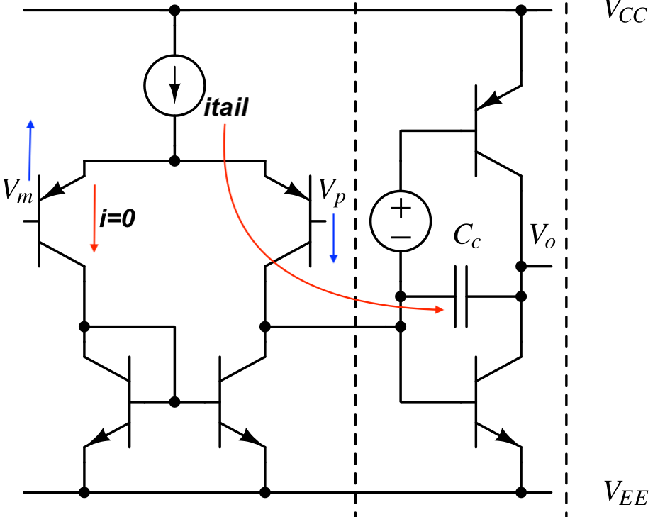
$$\text{SR}=\cfrac{I_{tail}}{C_c}$$
LSBW
LSBW (Large signal bandwidth) is the -3dB bandwidth achieved when output voltage is a significant value of the supply voltage. For example, in a +-5V supply opamp, if the output is 1Vpp, it can be called large signal. If the output is <100mVpp, it is called small signal.
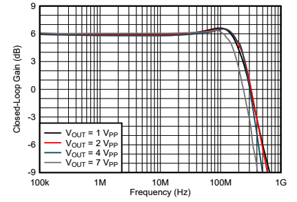
The large-signal bandwidth is constrained by the op-amp’s slew rate and other nonlinear effects. Producing a higher output amplitude requires a higher slew rate; if the slew rate is limited, the bandwidth decreases as the output voltage increases as shown above. To achieve a higher large-signal bandwidth (LSBW), amplifiers with a class-AB input stage are typically used.
SSBW
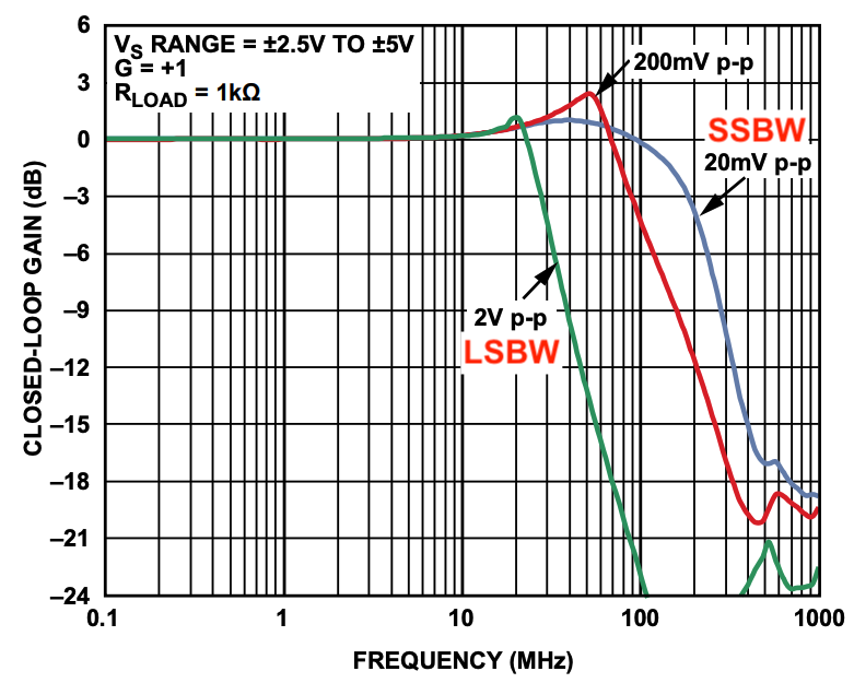
The small signal bandwidth shows the small signal equivalent bandwidth of the opamp. The output voltage is kept less than 100mVpp to keep the amplifier in its linear operating range. The behavior here captures the linear model behaviour of the amplifier.
SSBW Peaking and Phase margin
There is strong correlation between the phase margin and SSBW peaking of the opamp. Higher peaking means less phase margin and therefore less stability.
Input impedance
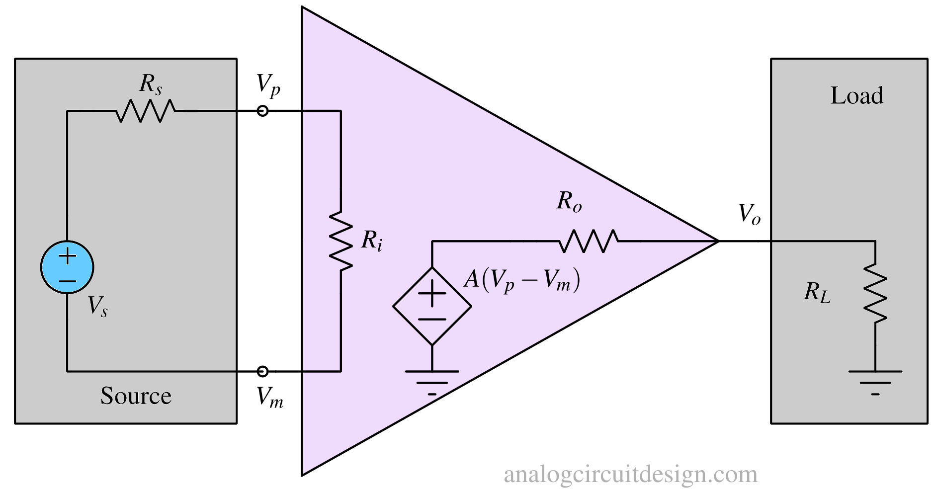
For an ideal opamp, the input impedance is considered infinite (Ri=∞). This is because we wish the opamp would not load the source circuit (Rs). In reality, value of Rs can be non-zero and a high-value. If Ri's value is near to Rs, voltage division happens and we don't get the desired signal level at the input. Usually, the input impedance it is very high in the order of > 106 Ω.

The input impedance depends mainly on whether the input stage of the opamp is FET-based or BJT based. If it is FET-based, the input impedance is greater than 1012 Ω. If it is BJT based input stage, then it could be in the order of 107 Ω.
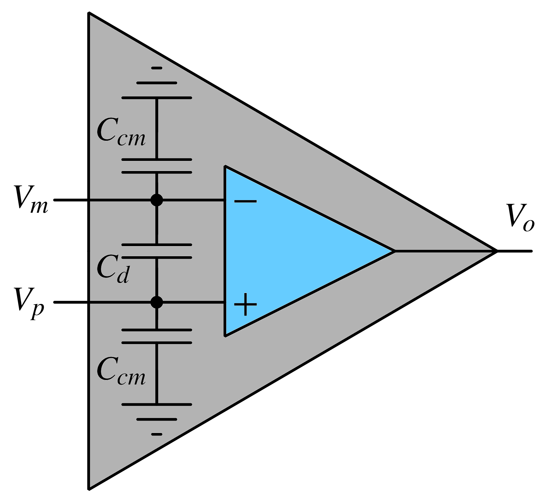
In the figure above, the Cd is the differential capacitor and Ccm is the common mode capacitor.
The impedance has a capacitive component as well. It varies from < 1pF to 20pF. Higher speed operational amplifier (GBP > 50MHz) should have input capacitance <5pF. Having lesser capacitance helps in G=+1V/V stability. To keep the capacitance low, high speed opamps have smaller input stage than precision op-amp. This is one of reason why high speed amplifiers can have lesser precision (Vos and CMRR). Precision opamps have bigger transistors to achieve very small offset voltage.
Output impedance
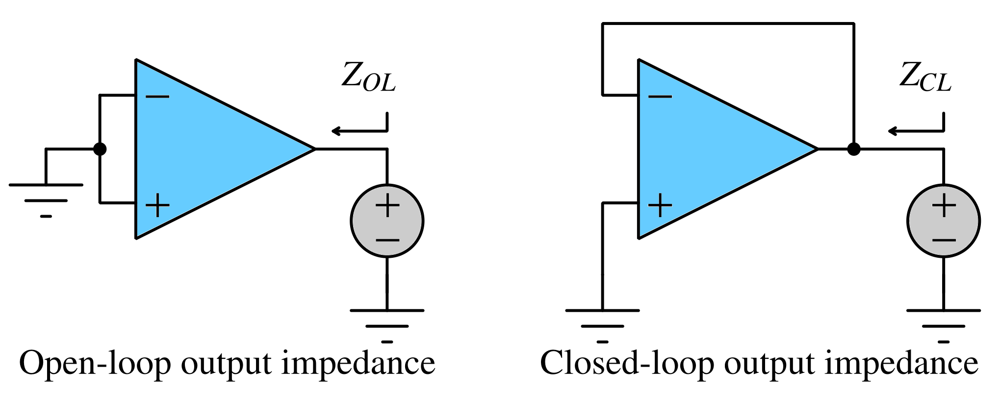
Usually, an opamp is considered a voltage source. Its function is to enforce a voltage on a load (RL). So, ideally, the output impedance of an opamp is zero (Ro=0). In reality, every voltage source has some resistance in series, which creates a voltage division and only part of the signal is enforced across the load.
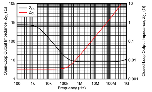
It can be observed from the above datasheet graph that the output impedance increases with frequency. This is happending because the gain of the opamp is falling with frequency as shown in gain-bandwidth plot. Only at some low frequency, the output impedance stays very low. In Sallen-Key filters, this can manifest as loss of attenuation at higher frequencies.
Input offset voltage
The input offset voltage is the difference between the inverting and non-inverting terminal of the opamp in the DC state. For an ideal opamp, this offset voltage should be zero. If there is an offset voltage at the input, that offset voltage multiplied by the huge gain of the opamp will saturate the output.
For unity gain opamp, the output is shorted to inverting terminal of the opamp. Usually, it is desired that the output is equal to the input voltage. However, due to offset voltage, the output is a few mV away from input voltage.
The input offset voltage should be low to make precise measurements. When measuring μV of voltage, the gain is set to be huge (>1000V/V). If mV of offset is present, we end up reading the offset of the amplifier rather than the input given to the amplifier. This is because the offset dominates the input signal.
Input bias and input offset current
Input bias currents are a characteristic of operational amplifiers (op-amps) and refer to the small currents that flow into or out of the input terminals of the op-amp.
Input offset current also known as input bias current imbalance, represents the difference in the bias currents between the two input terminals (inverting and non-inverting) of an op-amp. Input offset current can manifest itself as offset voltage if the magnitude of feedback resistor is high enough. `
BJT input stage

In the BJT input stage, the base current is required in the input transistors which allows the collector current to flow. The range of this current could be from a few nanoamperes to some microamperes. BJT input stage amplifier needs to be driven by sources having relatively low output impedances.
CMOS input stage
In the CMOS input stage, there is no input bias current because the transistors have an oxide barrier at the gate which is like an open circuit. These amplifiers are used to read out voltages where the source's output impedances are relatively high like sensors. Flicker noise of CMOS input stage (except chopper amplifier) is 10x worse than a bipolar amplifier. So for precision application where 0.1Hz-10Hz noise matters with decent speed, bipolar amplifiers are go-to solutions. However, bipolar amplifiers have high input bias currents.
The current noise of CMOS amplifiers is the lowest among BJT, JFET.
JFET input stage
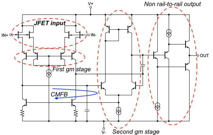
JFET provides a balance between CMOS and BJT opamps by eliminating the bias-currents and providing lower flicker noise than CMOS. In the above figure, JFET transistors are being used as buffer (common-drain/common-collector) configuration. It is driving a common-base stage creating a transconduction (gm). JFET-input amplifiers are used as test and measurement analog front ends, current sense amplifiers, analog-to-digital converter (ADC) drivers, photodiode transimpedance amplifiers, or as a multichannel sensor interface through multiplexers.
Noise in opamps
Real opamps contribute noise which limits the input sensitivity. There is signal level below which we cannot detect signals from a opamp because the output will be complete random noise signal. This lowest signal level is called noise floor of the opamp. The input stage of the opamp contributes more than 95% of the overall noise due to opamp. So, input stage selection is critical for noise critical applications.
There are two types of noise in opamps:
- Current noise
- Voltage noise
There are following types based on nature of noise generation and behaviour:
Thermal Noise (Johnson-Nyquist Noise)
This type of noise arises due to the random thermal motion of electrons within the resistors and semiconductor components of the op-amp. It is directly related to temperature and resistance and is characterized by a continuous spectrum of frequencies. Thermal noise is also known as white noise because it has a constant power density across the frequency spectrum. Mostly found in CMOS and JFET opamps, not in BJT opamps.
Shot Noise
Shot noise occurs when current flows throughout a PN junction. In BJT opamps, it is the dominant source of noise. The noise is modelled as a current which is temperature independent. However, due to the transonductance's temperature dependence, the input referred voltage noise due to shot noise becomes temperature dependent. In CMOS opamps, shot noise is not prominent.
It is also a white noise because it has a constant power density across the frequency spectrum.
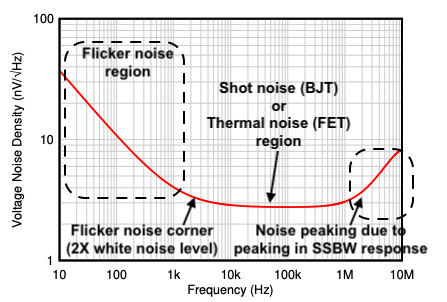
Flicker Noise (1/f Noise)
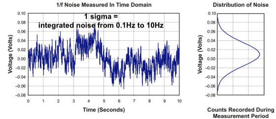
Flicker noise, also known as 1/f noise, is characterized by a spectrum where noise power increases as the frequency decreases. It is caused by dangling bonds near 2 dissimilar material junctions or semiconductor surfaces. Flicker noise can be particularly problematic in low-frequency precision applications. It is worst in CMOS amplifiers, moderate in JFET input opamps and best in bipolar opamps.
Burst Noise (Popcorn Noise)
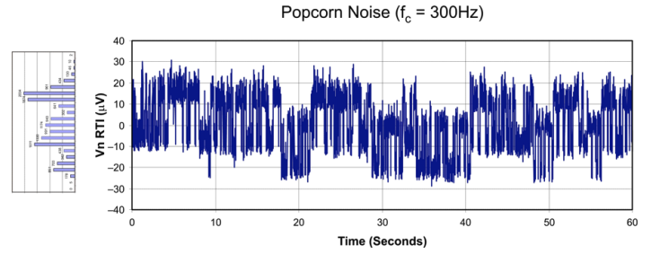
Burst noise consists of intermittent, sudden variations in voltage or current. It can be caused by defects in the semiconductor material and is more prominent at high frequencies. It appears as bursts of noise with random durations and amplitudes. It is found in all opamps.
Common mode rejection ratio (CMRR)
CMRR is a related parameter that specifies how well the op-amp rejects common-mode signals. It is expressed in decibels (dB) and represents the ratio of the differential gain (the gain for signals applied between the inputs differentially) to the common-mode gain (the gain for signals applied to both inputs simultaneously). A high CMRR indicates good common-mode rejection.
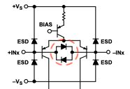
Common mode input range (CMIR)
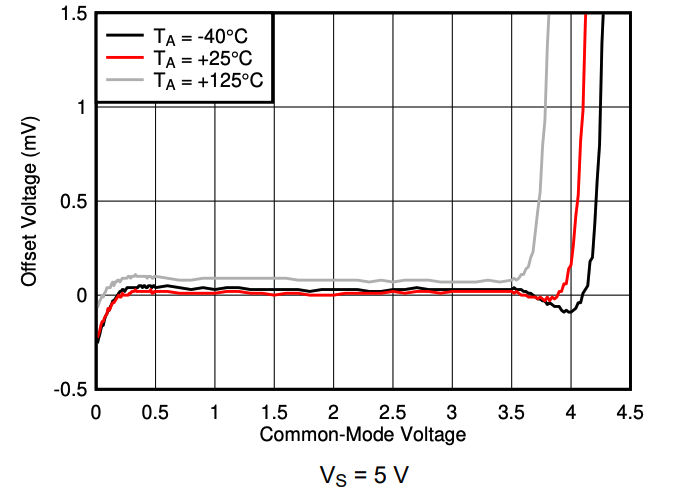
This specification defines the minimum and maximum voltages that can be applied to both the inverting and non-inverting inputs simultaneously while ensuring that the op-amp operates within its specified CMRR. In the datasheet of the opamp, we can find a plot where the input offset voltage is shown across input common mode. The point from where the input offset voltage starts taking off is the maximum common voltage which can be applied at the input of the opamp.

Within the amplifier, the common-mode input range (CMIR) is constrained by the tail PNP current source (Q3). As illustrated, the PNP input pair (Q1 and Q2) exhibits a base-emitter voltage drop VEB of 0.7 V, the PNP current source requires a minimum |VCE| of 0.2 V to operate properly, and there is an additional 0.2 V drop across the emitter degeneration resistor. Consequently, a total voltage drop of approximately 1.1 V (0.7 V + 0.2 V + 0.2 V) from VCC must be maintained to keep the current source active. At lower temperatures, VEB increases, thereby degrading the CMIR.
Output voltage and Claw curve
The output voltage headroom of an operational amplifier (op-amp) refers to the maximum voltage difference between the op-amp's output voltage and the voltage levels it can generate without distortion. The maximum voltage an opamp can theoretically reach is the supply voltage. However, in real opamps, depending on the architecture of the output stage of the opamp, output voltage never reaches supply voltage. There could be two type of architectures :
- Common emitter or Common source output stage (Found in rail-to-rail output stage amplifiers)
- Common collector or Common drain output stage (Found in non-rail-to-rail output stage amplifiers)
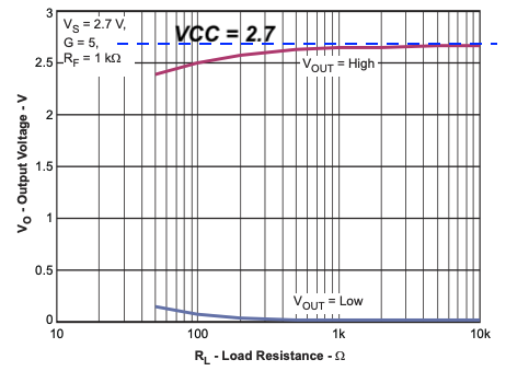
The voltage drop from VCC is called VOH (output-high). The voltage drop from VEE is called VOL (output-low). VOH and VOL are found using claw curve. The claw curve of an op-amp is a graph that plots the output voltage versus the output current (or load resistor), showing the limits of the output swing. It is named for its shape, which resembles a claw.
Common-emitter or Common source output stage
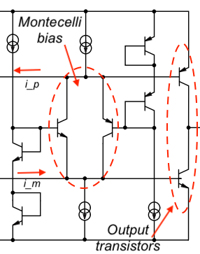
In the above figure, we can see that the output stage transistors are common-emitter configuration.
This allows the output to go less than 200mV near supply voltage. Output stage is basically a voltage controlled current source. The output stage quiescent current is decided by the Montecelli-biasing.
Common collector or Common drain output stage
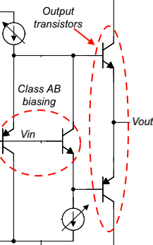
The output can go upto 0.7V + 0.2V = 0.9V (VBE+VCE,min) near VCC. For higher loads and lower temperatures, this drop can increase to 1.5V.
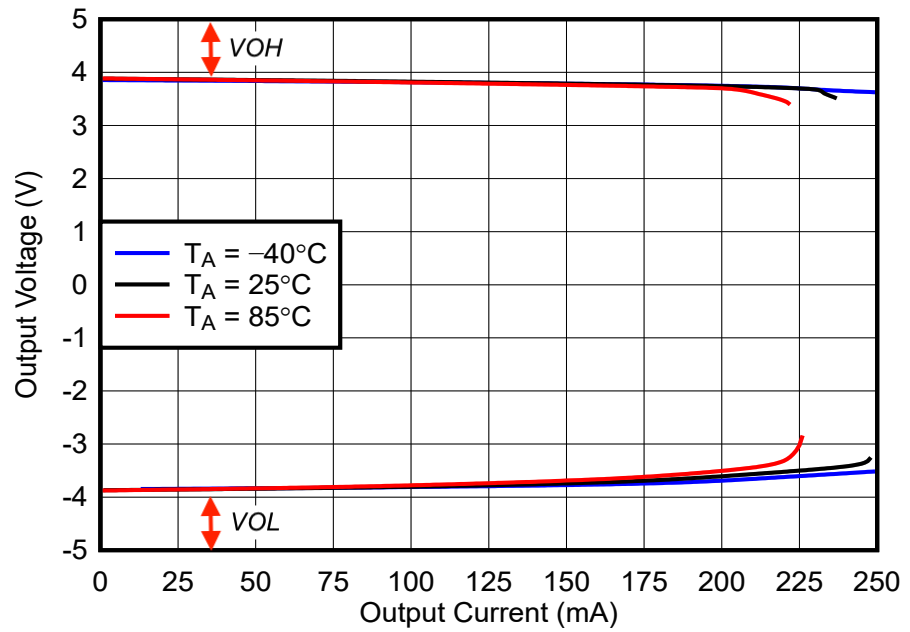
It can be seen from the above claw-curve plot of non-rail-to-rail opamp that the minimum VOH/VOL which can be achieved is 1V. It worsens with higher load current. Sometimes, datasheet show claw-curve as output voltage vs. current instead of load resistance.
Why choose non rail to rail opamp than rail-to-rail opamp ?
Non rail to rail opamps are usually more power efficient than rail-to-rail opamp for same bandwidth and noise. Suitable for multi-channel operations.
Power supply rejection ratio (PSRR)
The power supply rejection ratio (PSRR) measures the ability of an op-amp to reject variations in its power supply voltage, meaning it quantifies how well the op-amp can maintain a stable output when the power supply voltage changes.
The PSRR is measured as a ratio of the change in the input offset voltage (Vos) or output voltage (Vout) to the change in the power supply voltage (VCC or VEE), usually in decibels (dB).
$$\text{PSRR+}=20\log_{10}\left(\Delta{}V_{out}/\Delta{}V_{cc}\right)$$
$$\text{PSRR-}=20\log_{10}\left(\Delta{}V_{out}/\Delta{}V_{ee}\right)$$
Maximum input differential voltage
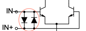
In a lot of amplifiers, there is a limit on the maximum differential voltage which can be applied across its two inputs.
The limit comes from protection diodes (as shown above) which are added to avoid breakdown of sensitive input differential pair. The breakdown can happen is fast large signal step when for a moment, a large differential voltage appears across the input pair. Also, during multiplexed operation, switching from one amplifier to another can cause large differential across the input pair. For closed loop negative feedback operations, it does not pose any limit however for multiplexed inputs, these amplifiers are not suitable.
There are amplifiers which do not have these differential limits called MUX-friendly input amplifiers. E.g., OPA828, OPA698. However, the impact is increased power consumption for same speed. Due to additional input stage transistors, the noise increases.
Distortion or THD
Distortion refers to the deviation of the output signal from the input signal. Op-amp distortion can affect the accuracy and fidelity of amplified signals in electronic circuits.
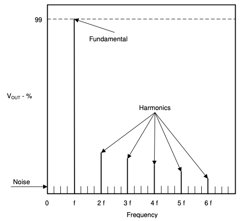
Distortion can be categorized into the following:
- Harmonic Distortion: Harmonic distortion is one of the most common types of distortion in op-amps. It occurs when the input is an ideal sinusoid and the op-amp introduces additional harmonics or frequency components at the output.
- Intermodulation Distortion (IMD): Intermodulation distortion occurs when two or more different frequency signals are present at the input of the op-amp. The op-amp can mix or modulate these signals, creating sum and difference frequency components that were not in the original signal. IMD can lead to the generation of unwanted spurious frequencies near the input signal frequency which are hard to filter out.
- Slew Rate Limiting: When an op-amp's input signal changes too rapidly, and the slew rate of the op-amp is insufficient to follow the input. If a high-frequency sinusoid is given at the input, the output waveform becomes triangular instead of sinusoid.
- Cross-Over Distortion: Cross-over distortion is specific to push-pull or complementary output stages of op-amps, such as those found in audio amplifiers. It occurs at the transition point when switching between the two output devices (e.g., transistors), leading to distortion near the zero-crossing point of the input signal.
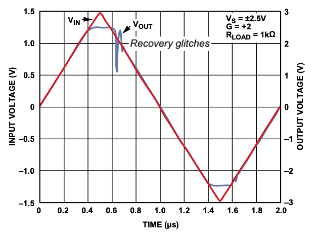
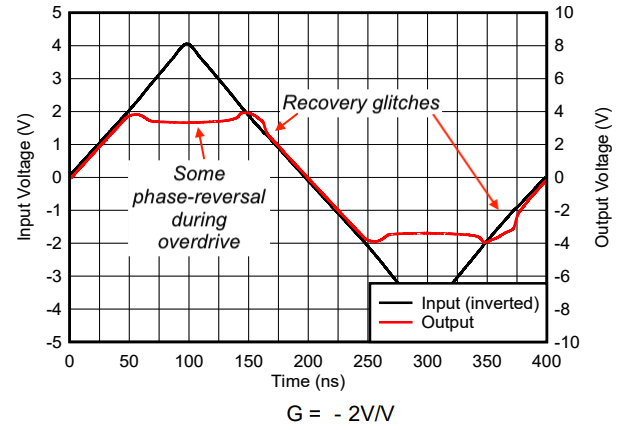
Overdrive recovery
Junction temperature
Maximum junction temperature is the maximum temperature at which the semiconductor can operate. Usually it is mentioned in the datasheet.
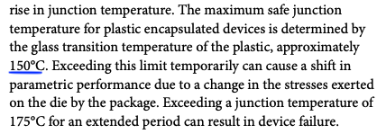
The junction refer to the PN junctions formations across the chip. If the chip junction temperature (Tj) exceeds the maximum junction temperature specified in the data sheet, a large number of electron-hole pairs will be generated in the semiconductor crystal, preventing the normal operation of the element.
The junction temperature is calculated using following formula :
$$T_j=T_a+R_{\theta{}JA}\times{}P$$
Where,
\(R_{\theta{}JA}\) is the thermal resistance between the junction and the ambient. The unit is °C/W. The \(T_a\) is the ambient temperature in °C. The \(T_j\) is the junction temperature in °C. The power generated by the opamp is represented using P (=V×I).
If using cooling (or thermal regulation) to control the case temperature, then the formula of junction temperature is :
$$T_j=T_c+R_{\theta{}JC}\times{}P$$
\(R_{\theta{}JC}\) is the thermal resistance between the junction and the case. The unit is °C/W. The \(T_c\) is the junction temperature in °C.
Example
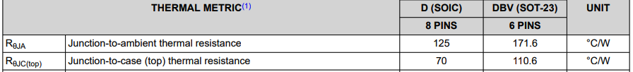
The thermal resistances are usually mentioned in the datasheet.
Question What is the junction temperature, if the supply of the amplifier is 10V, quiescent current is 10mA, ambient temperature is 25°C:
Solution The power produced by the opamp is :
$$P=10\text{V}\times{}10\text{mA}=0.1\text{W}$$
The case is held at ambient temperature so \(R_{\theta{}JA}\) is applicable. From the above figure, the value of \(R_{\theta{}JA}\) = 125 °C/W for SOIC package. So, the junction temperature is :
$$T_j = 25^o\text{C}+0.1\text{W}\times{}125^o\text{C/W} = 37^o\text{C}$$
Decompensated amplifier
Majority of opamps are unity gain stable. However, if you application requires something greater than gain of unity (e.g., gain of 5, 10 etc.), a decompensated amplifier is a more suitable option. A decompensated amplifier won't be unity-gain stable. However it will be stable for higher gains. A unity gain stable opamp will also work for higher gain, however the loop gain will be lower than a decompensated amplifier. Therefore decompensated amplifier provides better distortion and bandwidth for higher gain applications.
Let's compare between a unity gain stable amplifier with decompensated amplifier for high gain application.
| Properties | OPA859 | OPA858 |
|---|---|---|
| Compensation type | Unity gain stable | Decompensated (stable at G=7V/V or above) |
| Quiescent current | 20.5 mA | 20.5 mA |
| Supply Voltage | 3.3-5.25 V | 3.3-5.25 V |
| HD2 | -84 dBc | -98 dBc |
| HD3 | -78 dBc | -88 dBc |
| GBP (G=10) | 90 MHz | 550 MHz |